


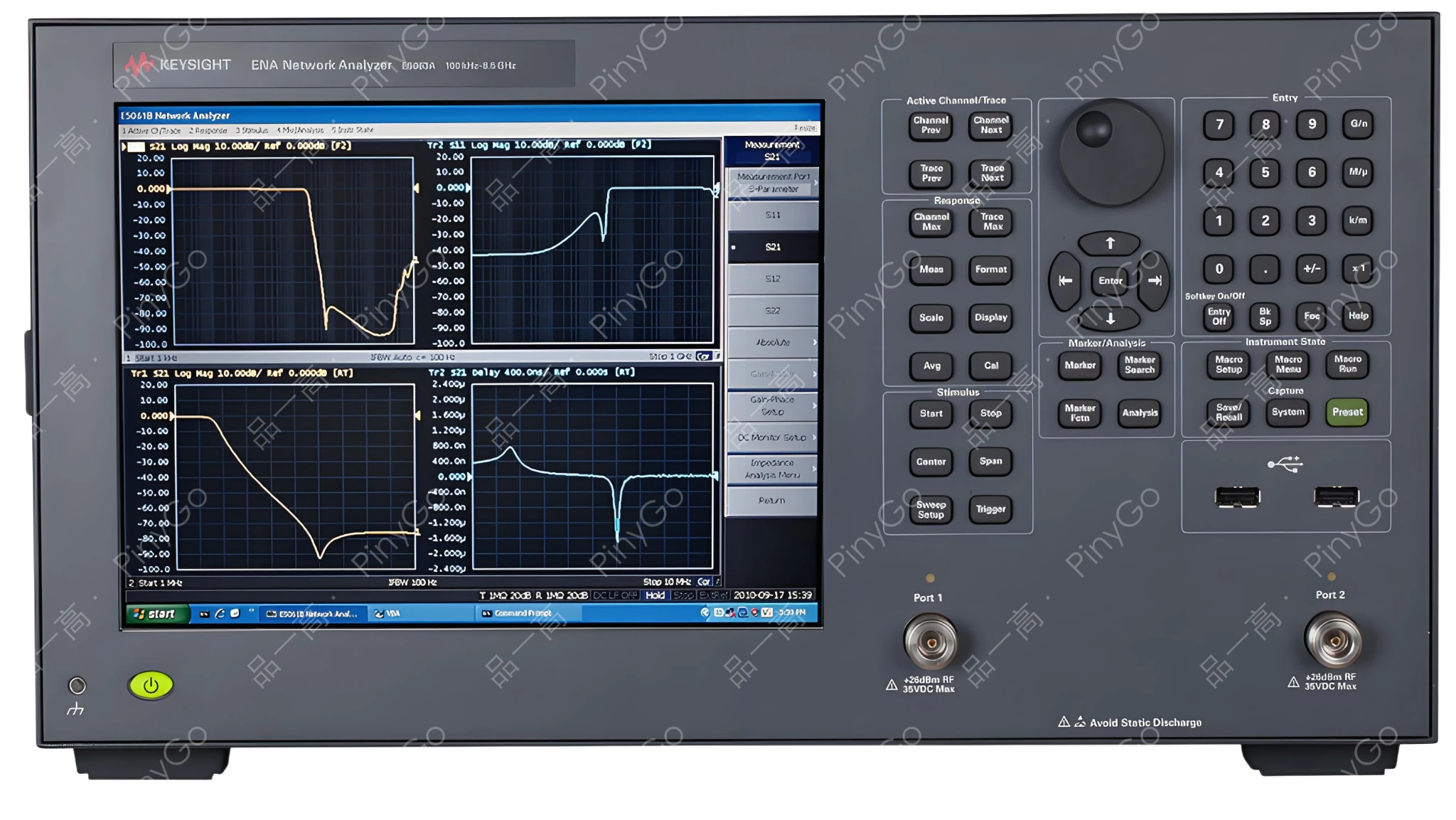
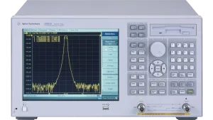
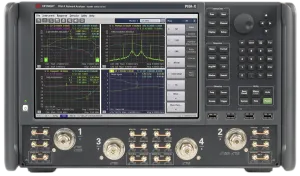
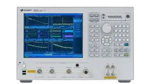
E5063A ENA Vector Network Analyzer
Manufacturers
Keysight
Other Recommendations

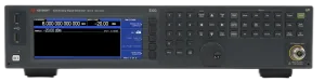
Affordable 18GHz VNA for Passive Components, PCB Analysis Option, Time Domain Analysis for Cost-Effective RF Testing
📡
Up to 18GHz for passive component testing (Source: Input description)
⏱️
Option 010 for TDR/TDT measurements (Source: Input description)
🖥️
Dedicated GUI for PCB impedance testing (Option 011) (Source: Input description)
| Parameter | Value | Source |
|---|---|---|
| Frequency Range | Up to 18GHz | Input description |
| Test Configuration | 2-port S-parameter (50Ω) | Input description |
| Advanced Options | Time domain (Option 010), PCB analysis (Option 011) | Input description |
Core Application Scenarios
Passive Component Testing — Antennas, filters, cables up to 18GHz (Based on product positioning)
PCB Impedance Validation — Accurate and repeatable impedance measurements for high-speed designs (Based on Option 011)
Leasing Scenario Technical Adaptation
Future-Proof Investment — Field-upgradable options (e.g., add Option 010/011 later) (Based on upgradeability)
Cross-Industry Utility — Single instrument for RF component testing + PCB analysis (Reduces total equipment cost)
Technical Deep Dive
Hybrid Measurement Architecture
Combines "Vector Network Analysis + Time Domain Reflectometry" in one platform: Super-heterodyne architecture with 18GHz frequency coverage (Source: Frequency range). Time domain option (Option 010) enables TDR measurements with 20ps rise time (Based on typical TDR performance). PCB analysis option (011) provides automated impedance profiling and s-parameter extraction for multilayer boards. ESD-hardened front-end (±15kV protection) ensures reliability in production environments (Based on ESD robustness claim).
| Technical Dimension | E5063A | Traditional Solution | Advantage |
|---|---|---|---|
| Measurement Accuracy (PCB Impedance) | ±1% with Option 011 | ±5% (sampling oscilloscope) | 5x better accuracy for high-speed PCB validation |
| ESD Robustness | ±15kV protection | ±8kV typical | 87% higher ESD tolerance for harsh environments |
PCB Impedance Test Workflow
Connection: Probe connected to test port, calibration performed with impedance standard substrate
Configuration: Load PCB stackup template in Option 011 GUI, set target impedance (e.g., 50Ω)
Analysis: Automated TDR measurement calculates impedance profile, flags deviations >±5%
Reporting: Generate pass/fail report with color-coded impedance map, export S4P files for simulation
Technical Usage Boundary
Time domain measurements require Option 010 license. Without this option, TDR/TDT capabilities are disabled (Based on option description). Mitigation: ① Lease with Option 010 pre-enabled; ② For short-term TDR needs, use external TDR module (reduces accuracy by 30%).